- HOME
- Wow! Cool Laboratory [Researcher Introduction]
- Katsuhiro Tomioka
Wow! Cool Laboratory [Researcher Introduction]
Division of Electronics for Informatics,
Research Group of Integrated Systems,
Integrated Electron Devices Laboratory
Research Center for Integrated Quantum Electronics
Fields of research: optical devices, semiconductor properties, compound semiconductors, CMOS, FET, nanowire, quantum structures, crystal growth
Research theme: Creating materials and technology platforms for non-flammable near-future devices
E-mail: tomioka[a]ist.hokudai.ac.jp
One-of-a-kind Crystal Growth Technology Paves the Way to Future Devices with Non-flammable LSI Circuits
The problem of heat generation in semiconductor integrated circuits has been solved with crystal growth technology that took many years to develop.
Semiconductor circuits that feature large-scale integration (LSI circuits) play the role of ‘brains’ in the smartphones, PCs, and digital home appliances that are now indispensable for smooth daily life.
LSI circuits perform various functions by integrating many elements, such as transistors (FETs) and capacitors, on a silicon semiconductor substrate. LSI circuits are becoming smaller and smaller year after year, along with the evolution of miniaturized devices demanded by the times, and researchers worldwide are competing to develop them (Fig. 1).
“However, the problem is always the amount of heat generated by the LSI circuit,” points out Katsuhiro Tomioka, associate professor at the Integrated Electronic Devices Laboratory. In viewing 4K video on a computer or smartphone, nearly 10 billion transistors inside the LSI circuit are simultaneously activated by the switching function to perform arithmetic processing.
“The heat generated by the LSI circuit is comparable to that generated at the nozzle of a rocket engine,” says Associate Professor Tomioka. “If a high-performance LSI circuit were mounted in a small device, such as a pair of eyeglasses or a watch, it would burn out. As a dramatic solution to this heat generation problem, we’ve been using the crystal growth technologies that we’ve accumulated over the course of many years to develop completely new ‘non-flammable semiconductor chips’.”
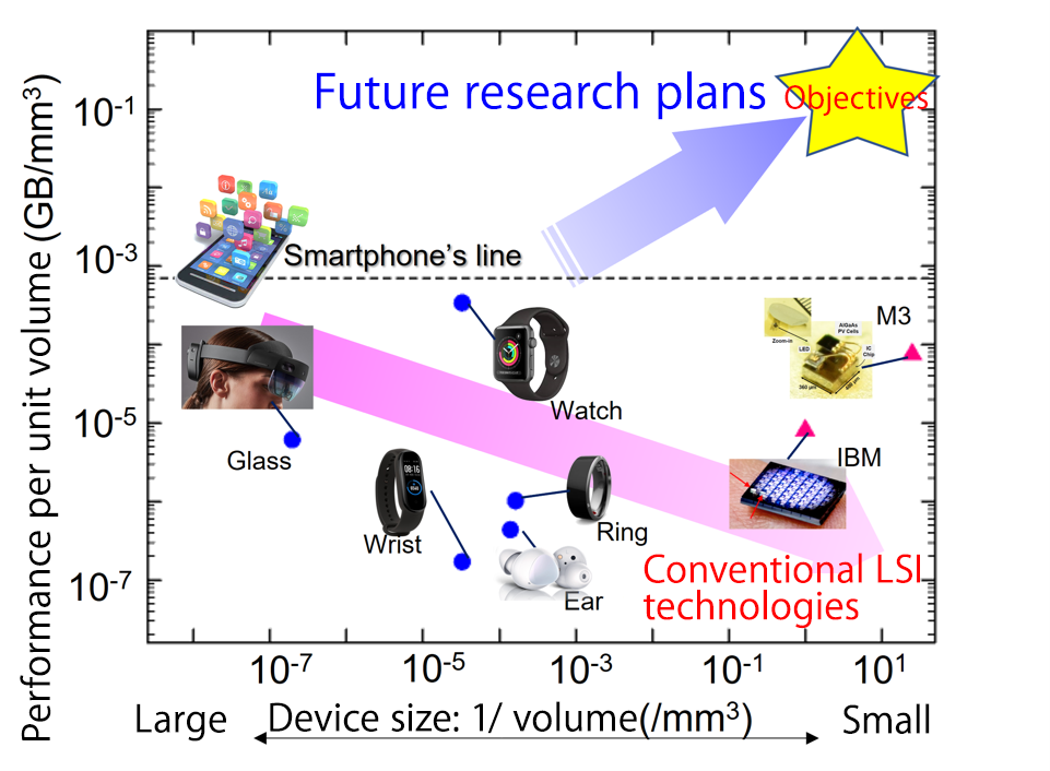
Fig1: Performance per unit volume benchmarks for small devices. The dashed line shows the performance and volume values for smart phones. The smaller the device, the more limited its functionality; the higher the functionality, the farther the device is from being a wearable size.
Construction of the world’s first compound semiconductor nanowire vertical transistor
The first thing that Associate Professor Tomioka did to achieve thermal control of the LSI circuit was to establish a technology that allows the flexible integration of III-V compound semiconductor nanowires made of various materials on a silicon substrate.
“Conventionally, when compound semiconductors made of various materials are grown on a silicon substrate, the result is not a uniform product that looks like the Japanese kenzan floral pin frog,” he says. “The pins on it point in many directions, and the product is considered to have poor performance. By combining top-down lithography technology and bottom-up crystal growth technology and by changing the atomic arrangement on the topmost surface of the silicon substrate with specific atoms, we’ve successfully integrated highly uniform, vertically freestanding III-V nanowires.” (Fig. 2)
Using the compound semiconductor nanowires constructed in this way, Associate Professor Tomioka and his colleagues went on to fabricate the world’s first vertical transistor (Fig. 3).
“LSI development has always involved a struggle for miniaturization and for solutions to heat generation problems,” he says. “By stacking FETs vertically, we’ve been able to reduce the LSI circuit’s footprint by 75%. And we’ve used a special structure called a modulation doped structure to create a path with less of the scattering that would otherwise impede the movement of electrons, thus enabling high current flow even at low voltages. We’re the only group in Japan that can fabricate these III-V compound semiconductor nanowire vertical transistors. We published on this technology in 2008 and have patented it.”
Surprisingly, this technique can be mastered by students in the Integrated Electronic Devices Laboratory in as short as three months. “When they look at the transistors they’ve made under the electron microscope, they’re surprised to see that they really can make them,” says Associate Professor Tomioka. “This strong impression seems to be what motivates the students in their research.” It’s evident that passing on this crystal growth technique, which can be performed by anyone, also leads to the fostering of young researchers.
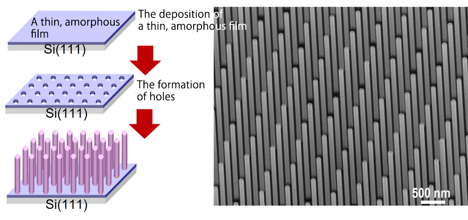
Fig. 2: When holes are made in a masking film on a silicon substrate and crystals are grown under specific conditions, GaAs nanowire arrays grow uniformly and vertically freestanding.
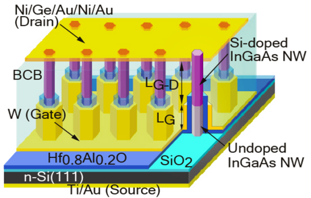
Fig. 3: Schematic of the vertical transistor structure
Unexpected tunneling effect cuts power consumption by the LSI circuit by 90%
In the process of fabricating compound semiconductor nanowire vertical transistors, the research group made an unexpected discovery.
“We discovered that a tunneling effect occurs spontaneously at the interface between the silicon substrate and the compound semiconductor nanowire,” says Associate Professor Tomioka. “This finding wasn’t intended from the beginning, but was entirely accidental. By utilizing the current generated by this electron tunneling effect in the switching element of the vertical transistor, power consumption can be reduced by more than 90% while simultaneously solving the long-standing problem of heat generation due to high power consumption by the LSI circuit.” (Fig. 4)
While discussions have already begun with manufacturers who are interested in this next-generation vertical transistor, Associate Professor Tomioka is also keen to create a technology platform that originates from Hokkaido University and centers on ‘non-flammable semiconductor chips.’
“We hope that venture companies will feel free to contact us about contributing to this new area of research, because it’s not something that requires large equipment or astronomical investment,” he says. “We now know that this technology can be applied to artificial intelligence circuits such as those in neuromorphic and reservoir computing. Then, the realization of the small, earphone-sized computers and high-performance AR devices seen in sci-fi movies will no longer be a distant dream. I’d like to keep on offering information from Hokkaido about how to create a new Japanese industry with free thinking that’s not bound by the conventional framework of silicon electronics development.”
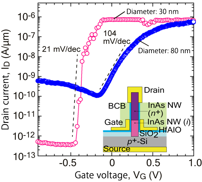
Fig. 4: The red line shows the behavior of an FET switching device that uses the tunneling effect. We proved that the physical limits of conventional MOSFETs can be overcome.
“When I was a student, my professor told me that crystals should be grown beautifully,” says Associate Professor Tomioka. “This is what led me deep into this field. I’d like to work with everyone to create a better future that will be realized through beautiful crystals.”