Application of topology in devices produces advancement of specification of ordinary devices and creates new functions that have never been realized yet
The most high transition temperature of superconductivity is about 160
K. On the contrary, transition temperatures of some CDW materials are higher
than the room temperature. Therefore, it is expected that realization of
the CDW quantum interference devices working at the room temperature. Conventional
medical SQUIDs have been used in large hospitals because they have to cool
down at low temperatures. The development of the room-temperature working
devices will provide more facile and more reasonable applications.
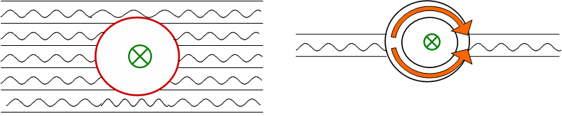
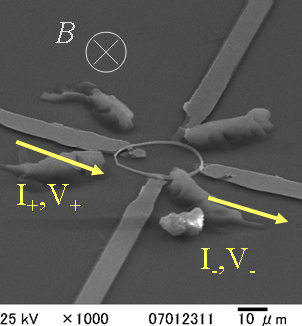
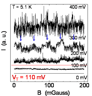
To prove this principle, our group investigate magnetic-field-dependence of conductivity at a charge density wave state experimentally. The left figure shows the scanning electron microscopy image of a ring-shaped crystal used for experiment. The ring of about 20 mm diameter is attached electrical contacts. The right figure indicates that the magnetic field dependence of current as applied voltage is constant. We discovered the conductivity periodically oscillates as a function of magnetic field the first in the world. (M. Tsubota et al., Reported at the 62nd Annual Meeting of Japan Physical Society.)
The single electron transistors needs ultra micro-fabrication and low temperatures because the Coulomb energy to excite one electron is enough higher than thermal fluctuation. (Or basically different approaches such as super-microparticle- or single-molecular-devices have to be carried out.) On the other hand, since the Coulomb energy is relatively large in the CDW systems, it is possible to realize such devices working at higher temperatures.
The single electron transistors have been expected for applications due to their super sensitive property. However they have worked only in laboratory yet. The topological soliton transistors will make a break-through.
“Nanotube” is now a common term referring to single-atom-thick crystalline sheets rolled into a cylinder of diameter 1-100 nm in a self-organizing manner. Carbon nanotube was first discovered in 1994, and instantly spotlighted as its cylindrical topology had bestowed distinct physical properties such as;
Besides carbon nanotubes, our group have been employing ourselves in synthesizing novel nanotube material with undiscovered properties. So far we have succeeded in synthesizing inorganic nanotube of layered materials having superconducting or charge-density-wave property, such as niobium diselenide (NbSe2) and magnesium diboride (MgB2). All our synthesis is based on gas-phase growth at rather low temperature up to 800 oC without the use of any catalyst. In contrast to high-energy conditions under the presence of catalyst particles, the mechanism of nanotube formation under these conditions is still unexplored and of wide scientific interest. One of our findings is that a ribbon-shaped nanofiber of NbSe2 voluntarily rolls itself into a tube when exposed to an electron beam (*). This useful behavior is attributed to the interaction between accumulated charge and the electron beam, and has the potential to develop into a technique to manufacture nano-structures with arbitrary shape. MgB2, whose superconductivity was discovered as recently as in 1999, are now considered promising material to form superconducting wire owing to its moderately high transition temperature of 39 K and good crystallinity. Undoubtedly MgB2 nanotubes, once a sufficient yield is attained, would be incorporated in a SQUID to fulfill spatial resolution unparalleled among conventional film-based SQUIDs.
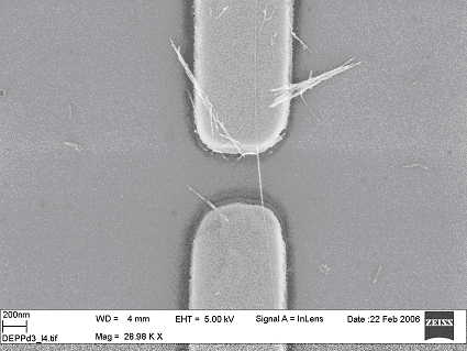
Figure 3: the nanotube sample controlled by dielectrophoresis method.
